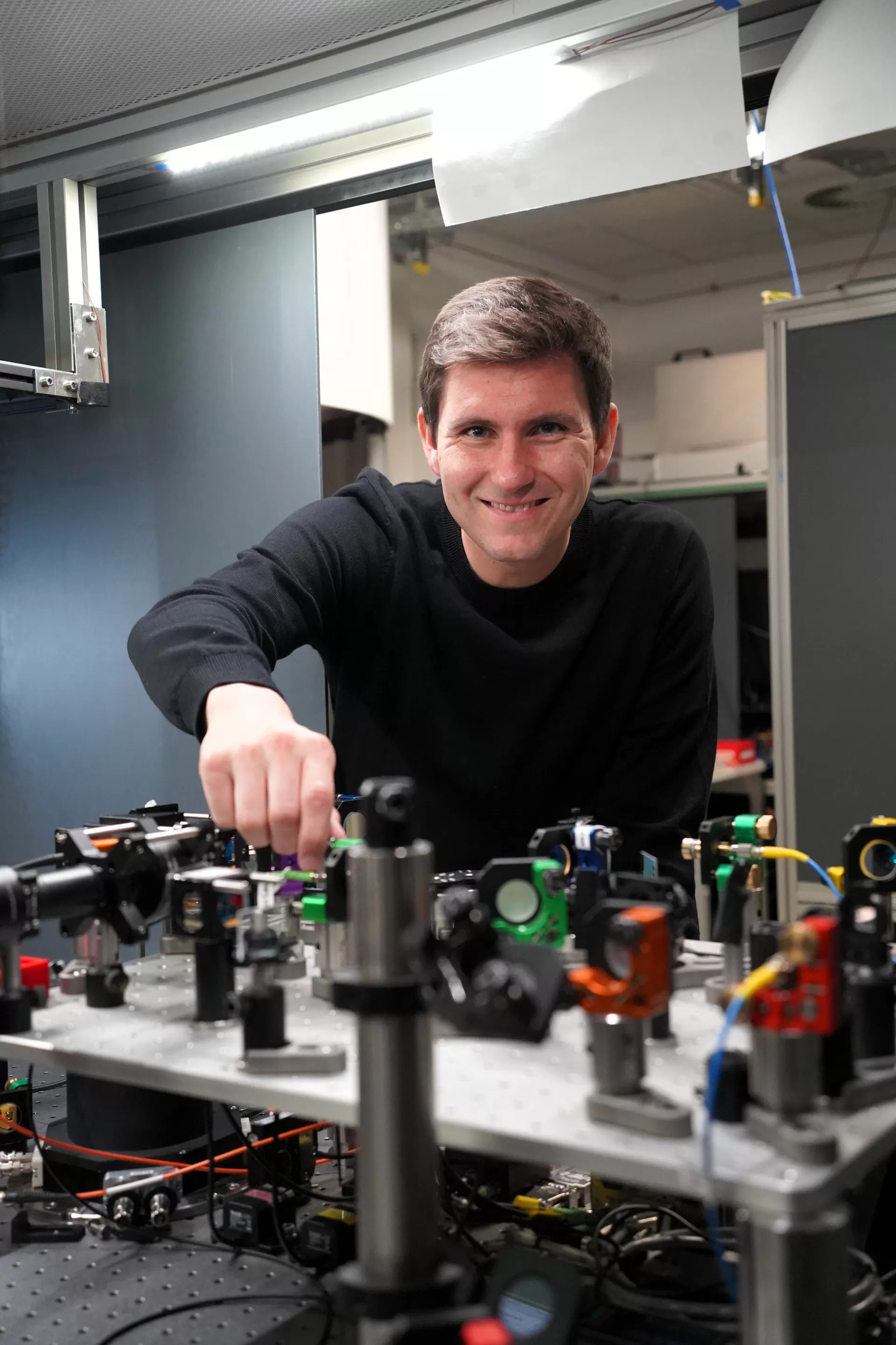
Nicholas Güsken
Understanding how light and matter interact at the nanoscale level is fundamental to many new technologies, especially quantum technologies. Physicist Nicholas Güsken combines basic research in quantum optics with engineering know-how. At the University of Paderborn he is developing the building blocks for photonic quantum technologies and quantum networks.
Nicholas Güsken is interested in controlling photons, the smallest energy packets in a beam of light. Photons have quantum mechanical properties and are able to exist in multiple states simultaneously, which makes them fascinating research subjects. A single photon can appear to travel down multiple paths at the same time, to oscillate in different directions, and even take on different colors simultaneously. It is only when photons are measured that a single, identifiable state emerges from this superposition of possible states. “If we deliberately combine several such quantum states, the amount of information we can represent about all possible states grows dramatically,” says Güsken, who was appointed Junior Professor of Quantum Photonics and Optoelectronics at the University of Paderborn in 2025. “This is where quantum computers have a major advantage over classic computers.”
Our goal is to control light at the nanoscale level.
Quantum photonics makes use of these quantum mechanical properties of light by generating, controlling, and linking individual photons in a targeted manner. “We manipulate atoms or atom-like quantum systems that emit photons and we integrate them as interfaces on chips, with the aim of harnessing quantum properties for communications, calculations, or sensor systems,” says Güsken. “Our goal is to control light at the nanoscale level.” In this way, Güsken is laying vital foundations for the quantum networks, computers, and measuring devices of the future – a future that will largely be built on light.
World-class nanofabrication
The quantum systems that Güsken is studying are integrated in optical circuits called single-photon sources. These are the key light-emitting building blocks of photonic quantum networks. Ions of the rare earth erbium are particularly promising single-photon sources. They emit light in the infrared region, i.e. close to the wavelengths that are already used for optical data transmission in glass fibers.
Researchers all over the world have been trying to use erbium as a quantum light source for some years now. “Erbium is a very stable single-photon source. We plan to integrate it into optical chips and optimize it to give it the desired optical properties,” says Güsken. “Our aim is to get erbium to emit indistinguishable single photons, almost at the press of a button, with frequencies we can actively control, allowing us to establish a source that can be used in quantum networks.”
Güsken conducted research into waveguides with integrated erbium back when he was a postdoc at Stanford University in California. By skillfully exploiting quantum effects, he succeeded in manipulating the environment around the erbium atoms so that the number of emitted photons increased dramatically. This is particularly important because erbium is a very weak light source. Temperature, crystal defects, electron fluctuation, and other factors can affect its stability, for instance altering the color of the photons it emits. In Paderborn, Güsken is now attempting to stabilize this “noise” by actively controlling the electromagnetic fields in the immediate vicinity of the integrated erbium ions, as well as trying to make their frequency adjustable.
We are basically running our own mini chip factory here.
To achieve this, he and his team are producing their own erbium samples, optimizing them with the help of computer simulations, and testing hypotheses and prototypes in their own optical lab. Thanks to the experimental facilities at the University of Paderborn, they are able to manufacture photonic chips with erbium atoms implanted in the waveguide, as well as other active nanophotonic platforms. “We are basically running our own mini chip factory here,” says Güsken. “These advanced nanofabrication and experimental characterization capabilities are absolutely essential for cutting-edge technology.”
A career lit by photons
Nicholas Güsken discovered an interest in light early on. After studying physics at RWTH Aachen University and nanomaterials science at Sorbonne University in Paris, he wrote his doctoral thesis at Imperial College London on integrated nanophotonics. This is a sub-field of optics and solid-state physics that studies how light can be manipulated at the nanoscale level. “Integrated nanophotonics is about manipulating light-matter interaction close to – and in some cases well below – the refraction limit,” says Güsken. It is possible to generate very strong interactions between light and fluorescent materials. Integrated nanophotonics can also make optical systems scalable, opening up far-reaching new technological possibilities that would not be feasible with classic lens-based systems.
I had to decide between money and love, and I chose what I love: science.
A foray into private enterprise, as the lead research and development engineer of a deep-tech spin-off from ETH Zurich almost derailed Güsken’s basic research ambitions, but a year or so later, he returned to academia – going to the prestigious Geballe Laboratory for Advanced Materials at Stanford University on a Leopoldina Postdoc Fellowship. “I had to decide between money and love, and I chose what I love: science,” says Güsken. “There is an extremely high concentration of very interesting people at Stanford who want to create something new and think in new directions – that’s what drew me.” Offers followed from Silicon Valley and from universities in the United States. Once again, he opted for science – and Europe.
From California to Paderborn – choosing cutting-edge research
Nicholas Güsken joined the University of Paderborn in 2025 because the Institute for Photonic Quantum Systems was being set up there. In Paderborn, around 140 academics from computer science, mathematics, electrical engineering, and physics conduct research on the latest questions in quantum photonics using excellent technical facilities. “Everything you need to build novel photonic quantum systems and conduct cutting-edge research is under one roof here,” says Güsken.
A grant from Wübben Stiftung Wissenschaft, support from the Returning Young Scholars Program of the State of North Rhine-Westphalia, and a tenure-track junior professorship made Güsken’s decision easier. The starting conditions and the offer from Paderborn were so attractive that he turned his back on California and rejected other tenure-track professorship offers in the United States. “The field of integrated photonics and quantum optics needs high initial investments because of the complex fabrication facilities and specialized equipment,” says Güsken. “This is where the University of Paderborn is in a strong position.”
In Güsken’s view, the university, where Germany’s first light-based quantum computer has been running since 2024, is on the right track to prosper in a competitive international environment, particularly with its clear focus on quantum photonics, quantum optics, and optoelectronics. “We are all independent researchers here, but we are traveling in the same direction, and that can produce all manner of good results,” he says. He himself intends to continue focusing on open-ended basic research alongside his more practical projects. “Like every researcher, I am eager to discover effects that we didn’t expect and to help expand our fundamental understanding of nature,” says Güsken.

Quantum physicist Nicholas Güsken has been a tenure-track Professor of Quantum Photonics and Optoelectronics at the University of Paderborn’s Institute for Photonic Quantum Systems (PhoQS) and Center for Optoelectronics and Photonics (CeOPP) since 2025. Previously, he worked as a postdoc at Stanford University and as lead research and development engineer for Swiss deep-tech company Polariton Technologies (now Marvell Technology, Inc.) in Zurich, a spin-off from ETH Zurich. He completed his PhD at Imperial College London, and studied physics, economics, and nanotechnology at RWTH Aachen University and Sorbonne University in Paris.